Overview
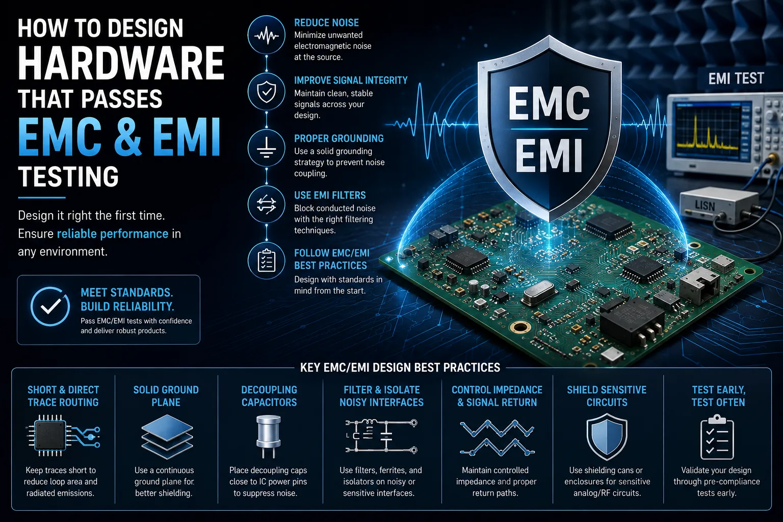
EMC/EMI testing asks two questions: does a product emit enough electrical noise to interfere with other equipment, and is it immune enough to noise from the outside world to keep working reliably? Failing either one late in a program is expensive — typically a PCB re-spin and a delayed certification date. EMC performance is decided almost entirely during layout and component selection, long before a board reaches a test chamber.
Grounding and Decoupling
A solid, unbroken ground plane is the single most effective EMC tool on a multilayer board — every high-frequency signal needs a low-impedance return path directly beneath it, and a split or slotted plane turns the trace into an unintentional loop antenna. Every IC power pin needs a decoupling capacitor placed as close as possible, with the shortest trace and via path to ground; a capacitor routed through a long trace loses most of its effectiveness at high frequencies regardless of its value.
Trace Routing and Filtering
Fast edge rates from clocks, switching regulators, and digital buses are the dominant source of radiated emissions, so keep these traces short, routed over a continuous ground plane, and away from board edges or connectors. Any cable or connector leaving the enclosure is both a potential antenna and a noise entry point — common-mode chokes, ferrite beads, and TVS diodes placed right at the entry point, not mid-board, are what actually suppress it.
Shielding and Testing Early
When layout and filtering aren't enough — high-power switching stages, RF sections, compact designs — a grounded shield with multiple low-inductance stitching points can contain what layout alone can't. Formal compliance testing is expensive and often booked weeks ahead, so pre-compliance testing with a near-field probe on an early prototype is worth doing: it catches the largest emission sources while there's still time to fix them with a layout revision instead of a full re-spin.
How PAK-EL LAB Can Help
PAK-EL LAB designs PCB layouts with EMC/EMI performance built in from the first stack-up decision — grounding strategy, decoupling placement, high-speed routing, and interface filtering — for embedded, industrial, and IoT hardware. If you're preparing a design for compliance testing, or have a board that failed and needs a targeted layout revision, our team can review the design and help get it through certification without a full redesign.
Related service: PCB Design