Overview
A PCB that works perfectly as a handful of prototype boards can still fail badly when it moves to mass production. Prototype quantities forgive a lot: a fabricator or assembler will often hand-fix a marginal footprint or missing test point on five boards without complaint. At production volume, the same issue means every panel gets flagged, every batch needs manual rework, and lead times stretch from days to weeks. Preparing a design for mass manufacturing is a distinct step from finishing the schematic and layout — it's the process of making sure the design, the documentation, and the physical panel are all ready for a line that can't stop to ask questions.
Design for Manufacturing (DFM) Review
A DFM review checks the layout itself against your fabricator's actual production capability, not the theoretical limits of the PCB technology. That means verifying trace width and spacing against their standard process (not their most expensive "advanced" tier), confirming drill sizes and annular rings are comfortably inside tolerance, and checking that copper-to-edge clearances and via-in-pad usage match what the fab line handles routinely. Small violations that a fabricator might quietly fix on a prototype order become panel-wide rejections at volume, because nobody is manually reviewing thousands of boards. Running a DFM check before Gerbers are released — not after the fabricator flags a problem — is consistently the cheapest point in the process to catch these issues; our guide to common PCB design mistakes covers many of the specific failure patterns a DFM pass should catch.
Design for Assembly (DFA) Considerations
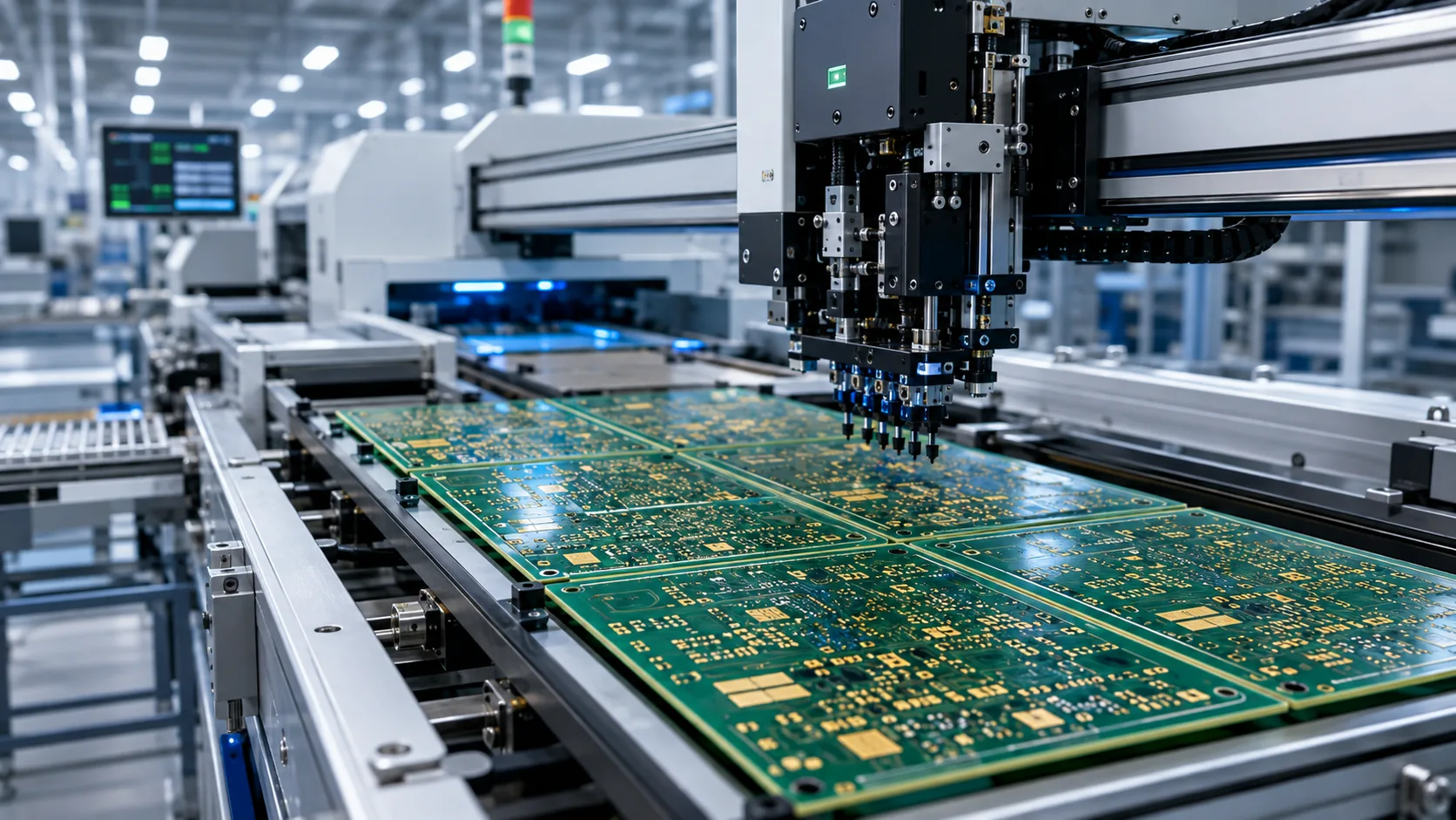
DFA looks at the same board through the assembly line's eyes rather than the fabricator's. Component placement needs enough courtyard spacing for pick-and-place tolerance, and mixing very fine-pitch parts with bulky through-hole connectors on the same side can force a slower, more error-prone assembly process. Footprint accuracy against the actual datasheet land pattern matters enormously at volume — a footprint that's "close enough" for hand-soldering ten prototypes will produce tombstoning or poor solder joints across an entire reflow batch. Orienting polarized components consistently (all diodes and electrolytic capacitors facing the same way, for example) speeds up both automated placement and any manual visual inspection step, and it's a detail that costs nothing to plan for at layout time but is expensive to fix once boards are populated.
BOM Optimisation
A bill of materials that was fine for building five prototypes from a distributor can become a bottleneck at production volume. Optimising the BOM for manufacturing means checking every part's actual stock and lead time at the quantities you need, not just its listing price, and specifying approved alternates for parts with single-source risk or long lead times. Reference designators, manufacturer part numbers, and package/footprint details need to be unambiguous — an assembler shouldn't have to guess which of three similar-looking resistors you meant. Consolidating part variants where possible (using one resistor value instead of three nearly-identical ones across a design) also reduces the SMT line's setup time and the chance of a placement error, which matters more as unit volume grows.
Panelisation and Test Point Planning
Individual boards rarely go through assembly one at a time — they're grouped into panels using tab-routing or mouse-bites, with fiducial markers for automated optical alignment. Panelisation decisions (panel size, spacing, break-away method) need to match what your specific assembly house's equipment handles, and this is worth confirming before layout is finalized rather than discovering a mismatch after boards are built. Test points for key power rails and communication signals should be planned into the layout from the start, not added as an afterthought — production test relies on accessible probe points, and retrofitting them onto a finished design usually means a re-spin. For boards headed into IoT products or other connected devices, planning for in-circuit test and functional test coverage at this stage catches firmware and hardware integration issues before they reach the field.
Production Testing Strategy
A testing plan built for mass manufacturing has to run fast and repeatably across every unit, not just verify that one board works. In-circuit testing (ICT) checks for shorts, opens, and correct component values immediately after assembly, catching solder defects before a board is ever powered on in its final configuration. Functional testing then verifies the board actually does its job — reading sensors correctly, communicating over its interfaces, drawing the expected current — under conditions close to real use. Boundary and burn-in testing, where boards run under load or through a temperature cycle before shipping, catches early-life failures that would otherwise show up as field returns. Deciding on this test strategy during design, rather than after the first batch comes off the line, is what keeps a production ramp from turning into a firefighting exercise.
How PAK-EL LAB Can Help
PAK-EL LAB prepares PCB designs for manufacturing as a standard part of our design process — DFM/DFA review, BOM optimisation, panelisation planning, and test point coverage, before files ever go to a fabricator. If you have a design moving from prototype to production and want a second set of eyes on manufacturability, our team can review it.
Related service: PCB Design