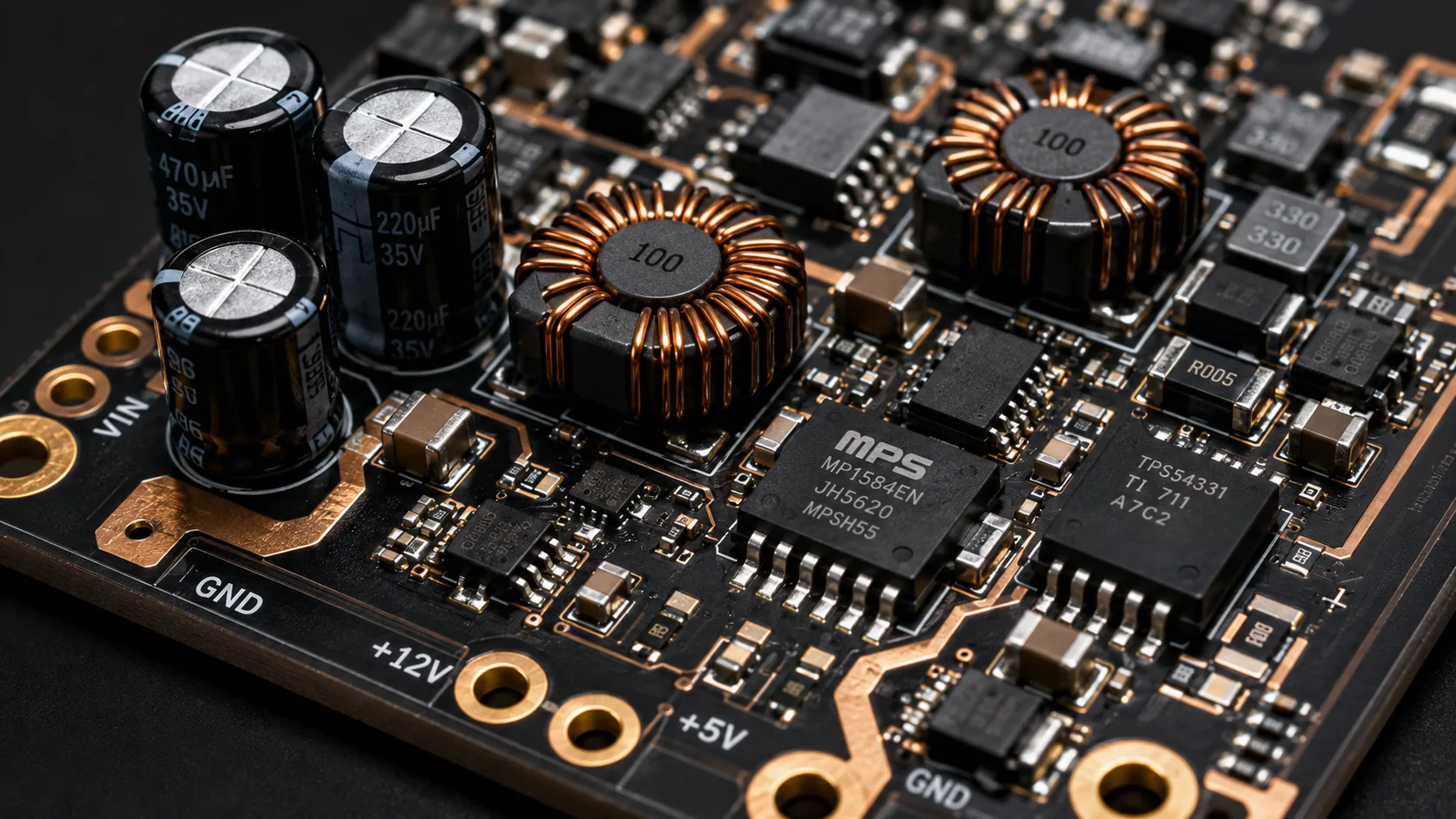
Overview
The power supply is the one circuit on a board that everything else depends on, yet it's often the last section designed and the first one blamed when a product misbehaves in the field. A microcontroller that resets under load, a sensor that reads noisy values, or a radio that drops packets when a motor kicks on are frequently power supply problems wearing a different symptom. Getting the power stage right — topology selection, regulator choice, charging strategy, and protection — is what separates a board that works reliably across its full operating range from one that only works on the bench.
Choosing Between Buck, Boost, and Linear Regulation
A buck (step-down) converter is the right choice whenever the input voltage is comfortably above the required output and efficiency matters — battery-powered products, anything running from a 12V or 24V rail, or systems where heat dissipation is a real constraint. A boost (step-up) converter is needed when the output voltage must exceed the input, which is common in single-cell battery products that need to generate 3.3V or 5V rails from a cell that sags well below that under load. Linear regulators (LDOs) are simpler, cheaper, and quieter from a noise standpoint, but they dissipate the voltage difference as heat — they're the right choice for low-current, noise-sensitive rails (analog references, RF supplies) rather than for dropping large voltages at meaningful current. Mixing switching regulators for the bulk power conversion with an LDO as a final "clean-up" stage ahead of a sensitive analog or RF section is a common and effective pattern; our PCB layout guidance covers the grounding and decoupling practices that make this combination work in practice.
Battery Charging Circuit Design
Battery charging is not just a matter of dropping in a charger IC — the charge profile has to match the chemistry. Li-ion and Li-Po cells need a constant-current/constant-voltage (CC/CV) profile with a precise voltage ceiling (typically 4.2V per cell), since overcharging degrades capacity quickly and, in the worst case, creates a safety hazard. NiMH packs use a different termination method entirely (negative delta-V or timeout-based). Beyond the charge IC itself, the layout and thermal design around it matter: charging at higher currents generates real heat, and a charger IC without adequate copper area for thermal dissipation will throttle its own charge rate or shut down under a full charge cycle. For portable products, a fuel gauge IC alongside the charger gives the firmware accurate state-of-charge data rather than relying on unloaded voltage, which is a poor proxy for remaining capacity under load — something we cover in more depth in our guide to reducing power consumption in battery-powered IoT devices.
Protection Circuitry
A power supply that works perfectly under normal conditions but has no protection against abnormal ones is a liability, not a finished design. Reverse-polarity protection (a series diode or, more efficiently, a P-channel MOSFET) prevents a swapped connector from destroying the board. Overcurrent protection — a polyfuse, a current-limiting regulator, or an active current-sense-and-shutdown circuit — contains a downstream short circuit instead of letting it cascade into the regulator or battery. Overvoltage protection (a TVS diode or crowbar circuit) matters most on inputs exposed to the outside world: automotive rails with load-dump transients, industrial 24V supplies with switching noise, or any connector a user might plug into an unexpected source. Input filtering — a bulk capacitor plus a small ferrite bead or common-mode choke — reduces conducted emissions and is frequently the difference between a board that passes EMC testing and one that needs a re-spin; our EMC/EMI design guide goes into the layout side of this in detail.
Thermal and Layout Considerations
Even a well-chosen regulator can underperform if the layout doesn't support it. Switching regulators need their input/output capacitors placed as close as possible to the IC with short, wide traces to minimize loop inductance and switching noise. The feedback trace on a switcher should be routed away from the switching node entirely — noise coupled onto feedback causes instability that's maddening to debug on the bench. Thermal vias under a regulator's exposed pad, sized and spaced per the datasheet, are what actually let the package dissipate heat into inner copper layers rather than relying on the small top-side pad alone. None of this is exotic, but skipping it is one of the most common reasons a power stage that simulates fine runs hot or unstable on real hardware.
How PAK-EL LAB Can Help
PAK-EL LAB designs power supply circuits — from simple LDO rails to multi-output switching supplies with battery charging and protection — as part of our embedded and PCB design work. If you're seeing field reliability issues that trace back to the power stage, or need a power architecture designed from scratch for a new product, our team can help.
Related service: PCB Design