Overview
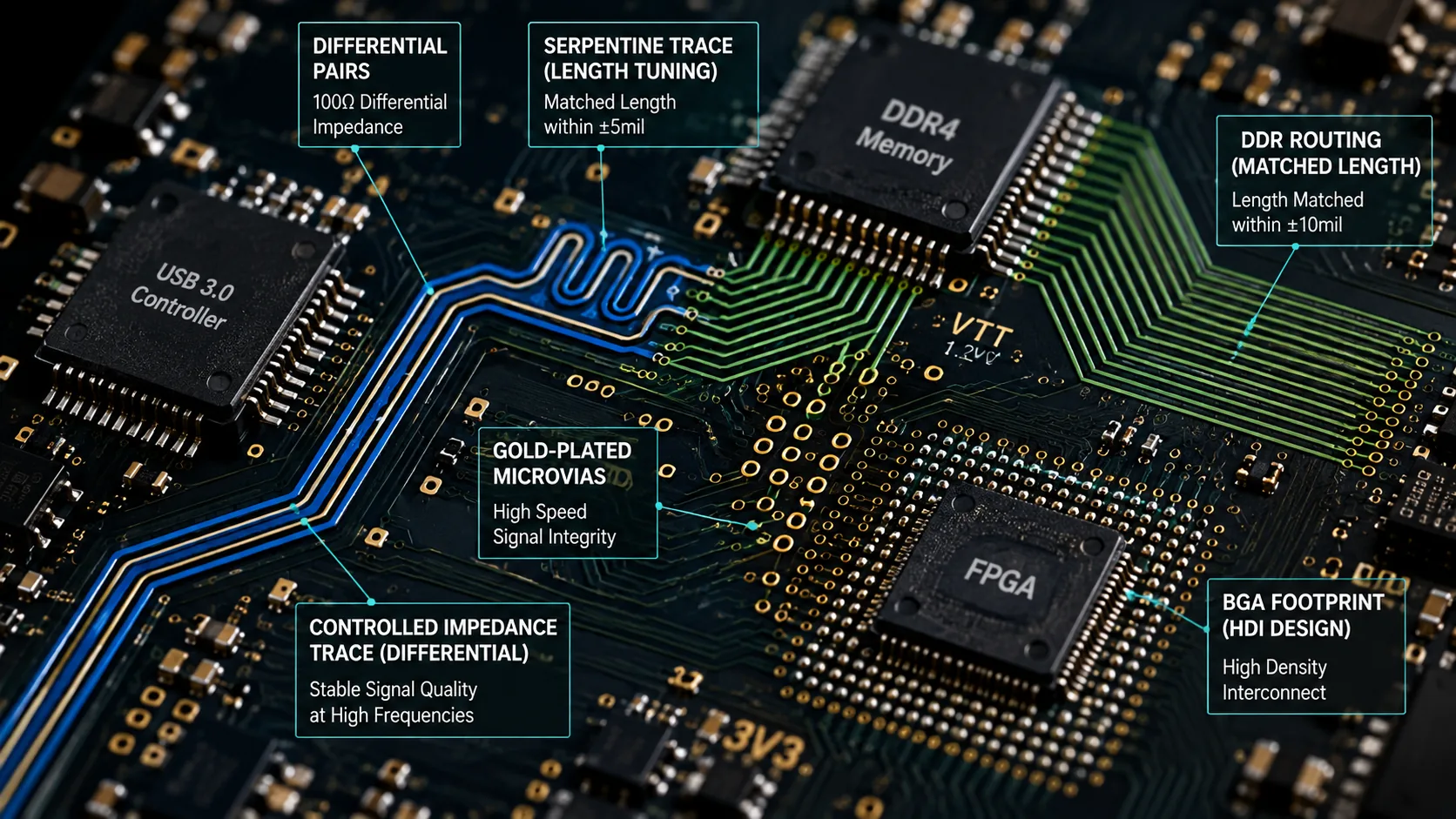
High-speed interfaces — USB 2.0/3.x, Gigabit Ethernet, and DDR memory — behave differently on a PCB than the slower digital signals most boards are built around. At these frequencies, a trace isn't just a copper connection; it's a transmission line with impedance, and getting that impedance wrong, or routing carelessly around it, causes signal reflections, timing errors, and EMI problems that are far more expensive to fix after fabrication than to design out up front. The core disciplines are the same across all three interfaces: controlled impedance, matched trace lengths, and a clean, uninterrupted reference plane.
Controlled Impedance Routing
Every high-speed interface specifies a target trace impedance — commonly 90Ω differential for USB, 100Ω differential for Ethernet and many DDR signals — determined by trace width, copper thickness, and the dielectric height to the nearest reference plane. Getting this right requires calculating stack-up parameters with a field solver or your fabricator's impedance calculator, not guessing at a trace width that "looks about right." A mismatch of even 10-15% from the target impedance causes measurable reflections at USB and Ethernet speeds, and DDR is even less forgiving given its tighter timing margins.
Stack-Up Planning for High-Speed Signals
A 4-layer stack-up with dedicated ground planes directly adjacent to each signal layer is close to the minimum for reliable high-speed routing — a 2-layer board simply doesn't offer the controlled reference plane these interfaces need. For DDR specifically, many designs use 6 or more layers to give address/command and data signals their own routing layers with solid, unbroken reference planes beneath them. Deciding layer count and stack-up early, as covered in our general PCB design tips, matters even more for high-speed work, since a stack-up change mid-layout usually means starting the critical routing over.
Length Matching and Skew Control
Differential pairs (USB D+/D-, Ethernet TX/RX pairs) need their two traces matched to within a small tolerance of each other — typically a few mils — to keep the differential signal clean and avoid common-mode noise that radiates as EMI. DDR takes this further: byte lanes and address/command groups need length matching across multiple traces, not just pairs, to keep data valid within the memory controller's timing window. Most PCB tools support length-matching rules and serpentine tuning traces for this; setting the rules before routing starts, rather than fixing skew after the fact, saves significant rework.
Via Usage and Reference Plane Continuity
Every via a high-speed trace passes through is a small discontinuity in its impedance, and every reference-plane split it crosses forces the return current to find a longer path — both increase reflections and radiated emissions. Keep via count low on critical high-speed traces, and where a signal must change layers, place a stitching via nearby so the return current has a short path back to the correct reference plane. Routing a differential pair across a plane split, even briefly, is one of the more common causes of an EMC compliance failure that only shows up in a test lab — a topic our EMC and EMI design guide covers in more depth.
Connector and Termination Placement
USB and Ethernet connectors need ESD protection and, for Ethernet, magnetics placed close to the connector with a clean, uninterrupted signal path — routing a high-speed pair around other components to reach a connector placed for mechanical convenience rather than signal integrity is a common layout mistake. DDR termination (series or parallel, depending on topology) needs to sit at calculated distances from the driver and receiver, not wherever board space allows. These are placement decisions, and like most PCB reliability issues, they're far cheaper to get right during floor-planning than to retrofit once routing is underway.
Simulation and Verification
For DDR designs especially, running post-layout signal integrity simulation — checking eye diagrams, timing margins, and crosstalk between adjacent traces — before committing to fabrication catches problems that are invisible on the schematic and hard to diagnose on a populated board. USB and Ethernet designs benefit from the same discipline at a smaller scale: verifying impedance and length-matching against the design rules before Gerbers go out, rather than discovering a marginal interface during bring-up when a board revision is the only fix.
Choosing Between Development Boards and Custom High-Speed Layouts
Many products prototype high-speed interfaces on a development board or module where the vendor has already solved the stack-up and routing problem, then move to a custom board once the design is validated. That transition is where high-speed layout mistakes are most common — a team confident with lower-speed custom boards can still underestimate what a controlled-impedance DDR or Gigabit Ethernet layout demands. Our comparison of custom PCB design versus development boards covers this tradeoff in more general terms, but for high-speed interfaces specifically, it's worth budgeting extra design and review time the first time a team moves an interface from a proven module to a from-scratch layout.
How PAK-EL LAB Can Help
PAK-EL LAB designs high-speed PCB layouts for USB, Ethernet, and DDR-based products, with stack-up planning, impedance control, and signal integrity verification built into the design process from the first schematic. If you have a high-speed interface design that needs an experienced second look, our team can review your stack-up and routing before fabrication.
Related services: PCB Design · Embedded Firmware Development